Diamond Heat Sinks and CVD Diamond Heat Spreaders

Diamond Thermal Management
DIAMOND THERMAL MANAGEMENT
Diamond Thermal Management Materials and CVD Applications
How Are Diamond Thermal Management Materials Used in High-Power Components?
Diamond thermal management materials leverage diamond's high thermal conductivity, electrical insulation, and low thermal expansion to shorten the heat-transfer path in high-heat-flux components. Alishan Diamond offers single-crystal diamond heat spreaders, polycrystalline diamond heat spreaders, copper-diamond composites, and CVD diamond heat spreaders that can be grown directly on silicon or silicon carbide substrates. The appropriate solution can be selected based on heat-source area, power density, package structure, and cost requirements.
Applications include AI/HPC, CPU/GPU/ASIC, GaN/SiC power devices, high-power LEDs, RF/microwave components, and laser diodes. These solutions support component designers in evaluating chip hot spots, package interfaces, and heat-spreader substrate configurations.
MATERIAL TYPES
What Are the Differences Among Single-Crystal, Polycrystalline, Copper-Diamond Composite, and Diamond Film Materials?
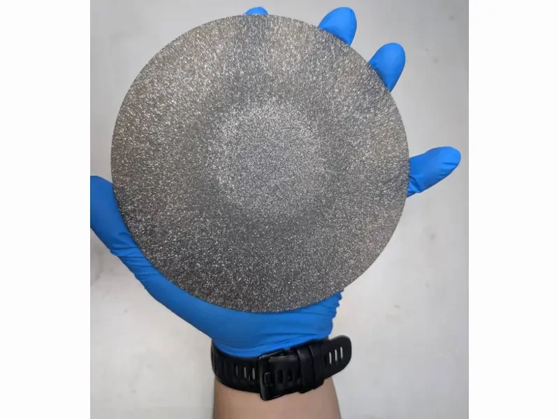
Polycrystalline Diamond Heat Spreaders
Thermal conductivity ranges from 1,000 to 1,800 W/m·K. Substrates with larger areas, such as 2-inch to 6-inch formats, can be produced, making them suitable for package applications requiring broad heat-spreading coverage and production-scale evaluation.
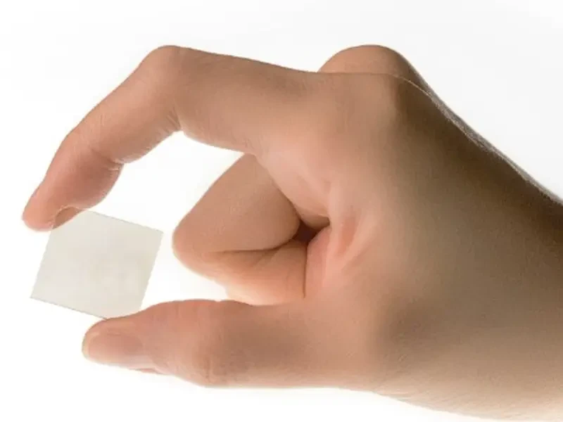
Single-Crystal Diamond Heat Spreaders
Thermal conductivity can exceed 2,000 W/m·K, making these materials suitable for small-area, high-power-density chips, high-power lasers, and components with stringent interface-quality requirements.
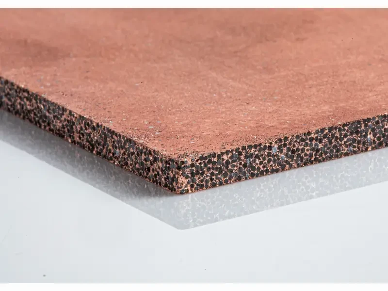
Copper-Diamond Composites
The copper-to-diamond ratio can be adjusted to balance thermal conductivity, electrical conductivity, and thermal-expansion matching. These materials are suitable for power modules and semiconductor package substrates.
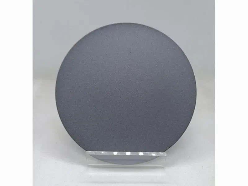
Diamond Films
DOSi and DOSiC processes integrate a diamond heat-spreading layer with Si or SiC substrates, shortening the heat-transfer path between the chip and the heat-spreading layer.
PROCESS CAPABILITY
Process Capabilities from CVD Crystal Growth to Package Interfaces
The process chain can include CVD diamond growth, precision cutting, grinding and polishing, planarization, surface metallization, and composite processing. These processes can support the production of diamond heat sinks and other thermal management components. Thickness, surface roughness, flatness, and metal-layer configuration can be discussed based on chip size, substrate material, and bonding method.
When evaluating thermal management materials, thermal conductivity should not be the sole comparison criterion. Interfacial thermal resistance, material thickness, coefficient of thermal expansion, bonding method, and the actual heat-source distribution also affect the component's final thermal performance.
TECHNICAL EVALUATION
What Information Is Required for Quotation and Technical Evaluation?
Please provide the heat-source dimensions, power or heat flux, allowable junction temperature, substrate material, finished dimensions and thickness, surface roughness, flatness, metallization or bonding requirements, samples, estimated quantities, and acceptance criteria.
Actual thermal conductivity, interfacial thermal resistance, and achievable machining tolerances should be confirmed according to the material grade, thickness, and test conditions.