
Diamond Lapping and Diamond Polishing Services
Diamond Lapping and Polishing
Lapping / Polishing / CMP / PMP
Diamond has the highest natural hardness (Mohs hardness 10). This is both its greatest advantage and its greatest processing challenge.
We specialize in precision diamond substrate lapping and polishing contract services, providing diamond polishing services for customers processing CVD or HPHT-grown diamond substrates to specifications ready for direct use in downstream applications such as semiconductors, optoelectronics, and quantum devices—without the need to invest in expensive in-house diamond precision processing equipment.
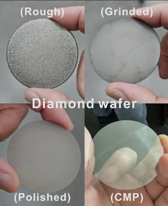
Our Core Processing Capabilities
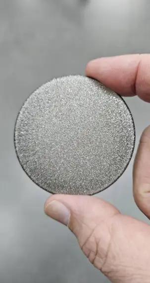
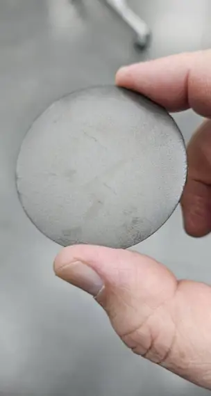
Rough Grinding Grinding / Lapping
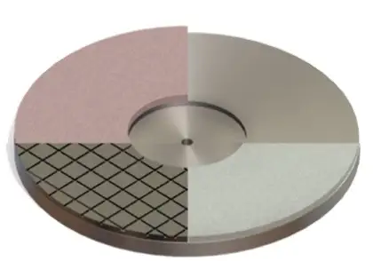
- Our diamond grinding services remove the rough surface structure and thickness variations of as-grown diamond, while adjusting the substrate’s initial thickness and flatness.
Fine Polishing Polishing
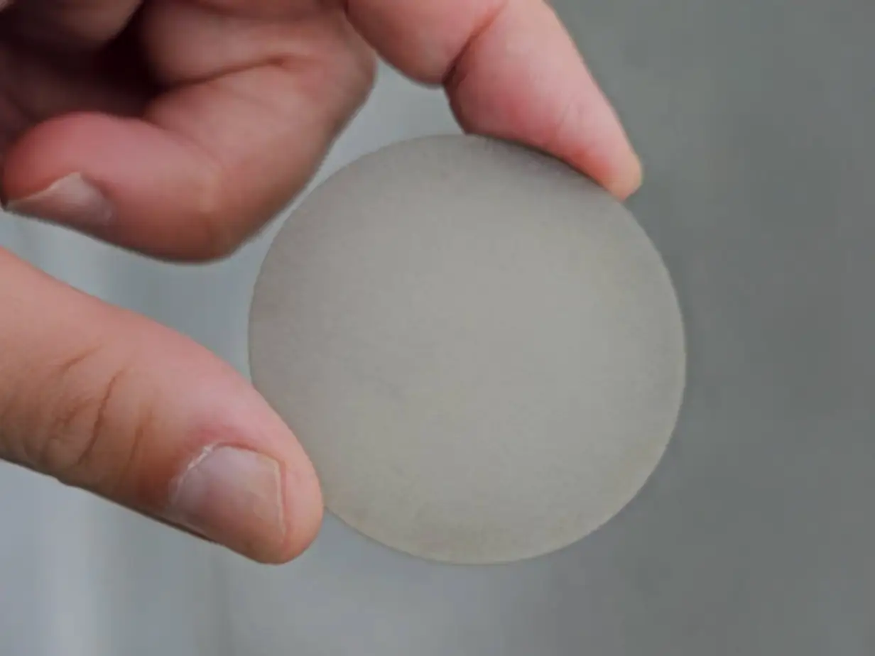
- Our diamond lapping and polishing processes use mechanical polishing, laser polishing, and other techniques to reduce surface roughness to the sub-nanometer level while eliminating subsurface damage, ensuring that subsequent thin-film deposition and device performance are not affected.
Chemical Mechanical Planarization CMP|Chemical Mechanical Planarization
- Combines chemical etching and mechanical polishing to achieve wafer-level flatness and low defect density, meeting the most stringent substrate flatness requirements of semiconductor and quantum devices
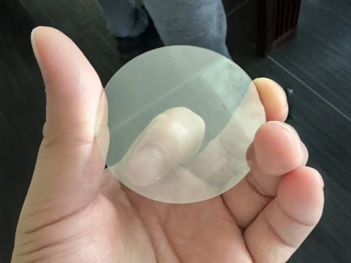
Plasma-Assisted Mechanical Polishing PMP|Plasma-Assisted Mechanical Polishing
- First uses plasma treatment to weaken the bonds on the diamond surface, then combines it with mechanical polishing to significantly improve processing efficiency and reduce subsurface damage, overcoming the efficiency limitations of conventional mechanical polishing for ultra-hard materials
Value-Added Services
Applications
Why Choose Us
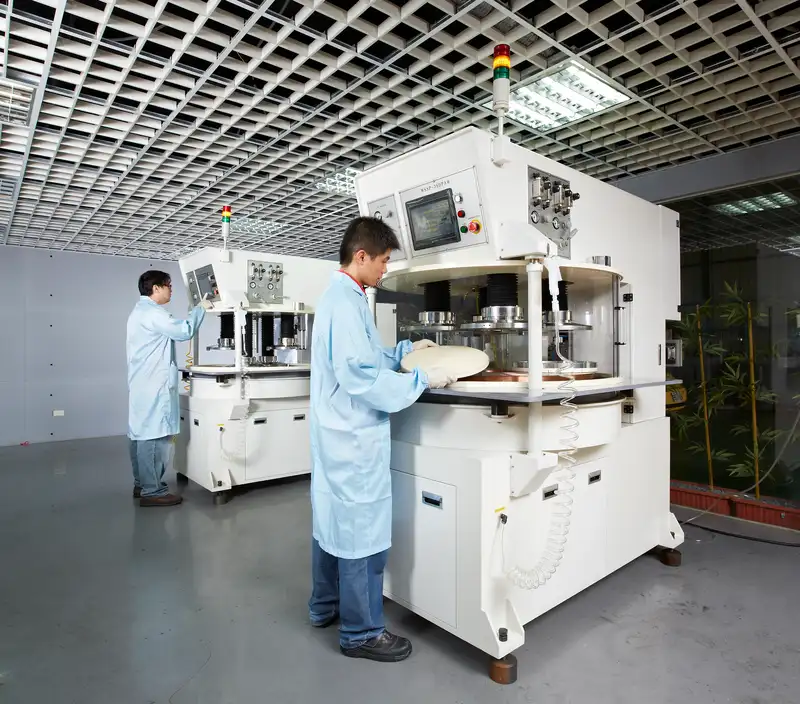
As a diamond grinding manufacturer and diamond polishing factory, we provide one-stop contract diamond substrate surface processing services, from rough grinding to precision CMP/PMP polishing, allowing customers to focus on their own product development without taking on the substantial investment and technical barriers associated with precision diamond processing equipment. Whether for single-crystal or polycrystalline diamond substrates, we provide surface processing tailored to specific application requirements.
Contact us to learn more about diamond substrate lapping, polishing, CMP, PMP, and customized contract processing services.
Discuss Your Customized Solution